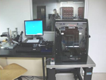
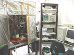
The Micro and Nanofabrication Service (MiNa) of the Institute of Micro and Nanotechnology (IMN) has a consolidated experience in the development of nanotechnology in Spain and belongs to the Network of Laboratories and Research Infrastructures of the Community of Madrid. MiNa has ISO 9001:2015 quality certification, working with great efficiency in its goal of meeting the growing demand for the manufacture of structures for clients outside the IMN.
It is worth mentioning about this service:
- Carrying out work beyond the standards, where our experts adapt nanotechnology, in a flexible way, to the most particular (and demanding) needs of the client,
- High resolution electronic lithography, (EBL)
- Offering ultra-high resolution ion beam (FIB) lithography in macroscopic areas,
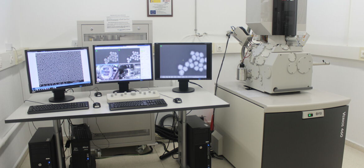
- Scanning electron microscopy (SEM) ” , both in the experience of the staff and in the capabilities of the equipment.
The service completes its objectives by transferring its experience to the rest of the Spanish scientific community by offering its knowledge and high-level infrastructure to R&D centers and technology companies.
Micro and Nanofabrication Service
To apply for any MiNa service, it is essential to send a request through the single reception method by sending an email to:
mina.imn@csic.es
subject: [Especificar el servicio requerido]
message: [Description of work to be performed and other requirements of dates, etc…].
Any service request that is not made through this single entry will not be honored.
Manufacturing techniques
Litografía de ultra-alta resolución por haz de electrones:
Resolución típica de 50 nm.
Equipo: Basada en SEM (LEO 145). Cátodo caliente de W o LaB6, Energía del haz: 25 KeVs.
Generador de estructuras: Elphy-Plus (2 MHz) con software para alineamiento con estructuras previas y para corrección de proximidad de estructuras. Editor gráfico de estructuras GDSII.
Portamuestras dotado de interferometría LASER que permite empalmar campos de escritura de 100 x 100 μm2 con un error < 60 nm. Área máxima de trabajo: 4×4 cm2
Litografía UV de Alta Resolución:
Resolución típica de 1 μm.
Ataque de ultra-alta resolución por haz de iones focalizado (FIB):
Resolución típica de 15 nm.
Equipo: ionLiNE (RAITH GmbH). Fuente líquida de Ga. Energía del haz: 30 KeVs.
Generador de estructuras: Elphy-Plus (2 MHz) con software para alineamiento con estructuras previas y para corrección de proximidad de estructuras. Editor gráfico de estructuras GDSII.
Portamuestras: dotado de interferometría LASER que permite empalmar campos de escritura de 100 x 100 μm2 con un error < 40 nm. Area máxima de trabajo: 10 x 10 cm2.
Otras características: dotado con un sistema de inyección de gases (GIS) que permite la deposición selectiva de SiOx, Pt, y Mo, con resolución de 50 nm. Dotado de un portamuestras especial (3D) que permite fabricar en 3 dimensiones.
Ataque seco por plasma reactivo (RIE):
Resolución típica de 0.8 μm.
Ataque húmedos y Limpieza
Deposición de dieléctricos por PECVD
Deposición de Metales por Pulverización Catódica y Haz de Electrones